






Silicon Wafer
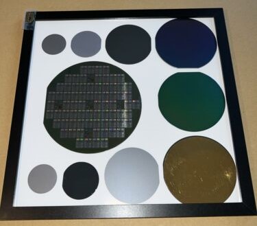 Silicon Wafer In electronics, a wafer (also called a slice or substrate) is a thin slice of semiconductor, such as a crystalline silicon (c-Si, silicium), used for the fabrication of integrated circuits and, in photovoltaics, to manufacture solar cells.
The wafer serves as the substrate for microelectronic devices built in and upon the wafer. It undergoes many microfabrication processes, such as doping, ion implantation, etching, thin-film deposition of various materials, and photolithographic patterning. Finally, the individual microcircuits are separated by wafer dicing and packaged as an integrated circuit.
.jpg)
.jpg)
.jpg)
.jpg)
.jpg)
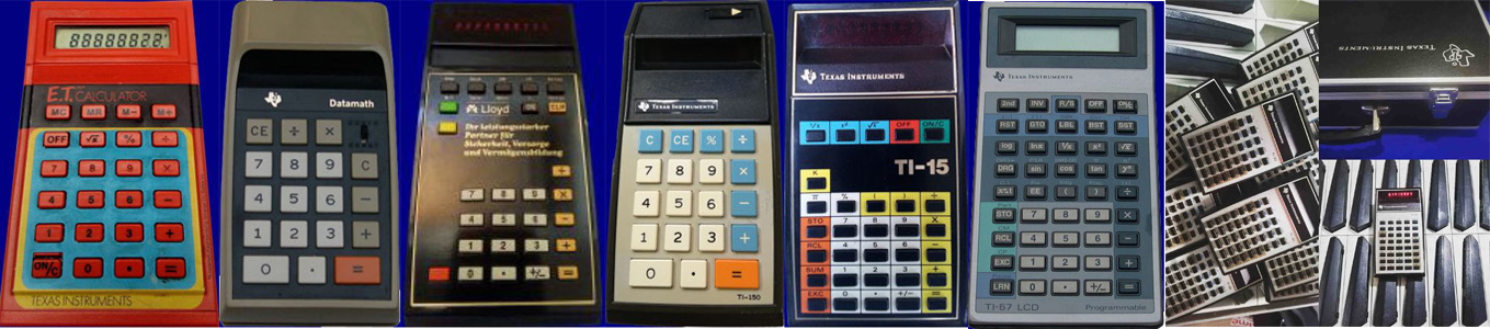
Here you can see some production scraps. The first photo (left) shows the component ready to be assembled, the second shows the various chips ready to be removed from the tray and placed in the ceramic chip. The three remaining photos show the various chips ready to be cut. I have to thank Francesco for giving me the opportunity to show these pieces!
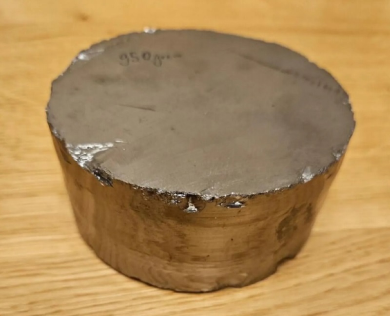
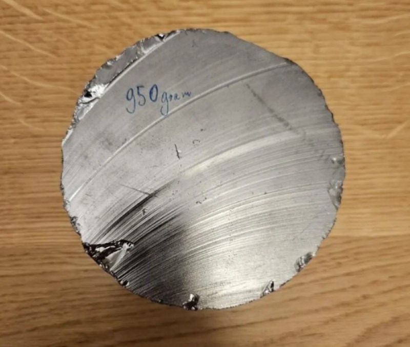
This 950g crystalline (105 x 50 mm) silicon ingot is a high-purity, technical-grade sample produced using the "Czochralski method" a technique commonly employed in the manufacture of semiconductors and microchips. It originates from Silicon Valley (USA), with final processing carried out in Poland. Silicon fragments in this form are rarely available outside of industrial manufacturing settings, making this item an exceptional collector's or display piece. Its metallic luster and regular crystalline structure make it ideal for scientific demonstrations, educational activities, and materials research.




.jpg "Core Module Watch")


.jpg "APPLE")
.jpg "Calculator Fuller")

.jpg "Console / Games")
.jpg "Olivetti Valentine")
.jpg "Battle Star Galactica")


.png)